先進製造與封測設備
Advanced Manufacturing & Packaging Equipment
Array Field of View × Nanometer Precision: A High-Efficiency Inspection Solution for Next-Generation Packaging
Technical Features
Array-based high-precision simultaneous scanning with expanded field of view improves efficiency by 4 to 10 times, addressing the production bottleneck in high-precision inspection (e.g., semiconductors).
Technical Description
Although commercial white light interferometry (WLI) systems are the mainstream solution for inspecting components smaller than 10 μm, their single-lens, small field-of-view architecture limits inspection speed, making it difficult to meet mass production demands and becoming a bottleneck for adopting high-precision processes. To overcome this limitation, this technology pioneers a MEMS-based miniature array white light interferometry module, introducing a parallelized array concept. It is applied in fields such as semiconductors, advanced packaging, and μLEDs to achieve multi-channel synchronized scanning, improving efficiency by 4 to 10 times while maintaining nanometer-level precision comparable to single-lens systems.
Coupled with an AI adaptive signal processing algorithm, it effectively compensates for inter-channel noise and signal variation. By incorporating off-axis optical lever design and real-time focus control, the coplanarity of lenses is precisely aligned to within 1.29 μm, enabling synchronized multi-lens scanning. The system achieves nanometer-level measurement accuracy (<10 nm) and a 4× larger field of view (1.2 mm × 1.2 mm), enabling simultaneous large-area, high-precision measurements.
Overall, this system breaks the trade-off between field of view and precision, offering a key solution for next-generation high-speed nanometer-scale inspection.
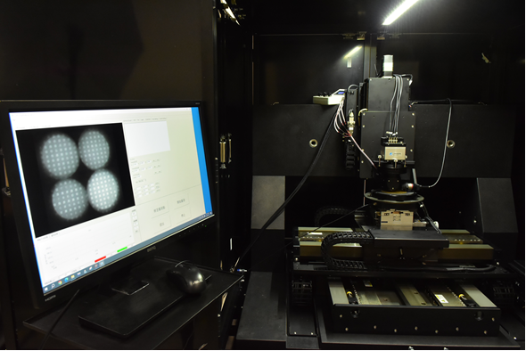
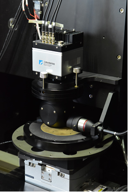
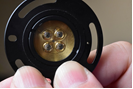
Photos
Contact
Name:李政韋
Phone:06-3847498
E-mail:bensonli@itri.org.tw