
化合物半導體與車用應用
Compound Semiconductors & Automotive Applications
GaN on X-Substrate Epitaxy & Process Technology
Technical Features
Specializing in heterogeneous GaN epitaxy on X-substrates, offering customized process and verification services to accelerate product development timelines.
Technical Description
Focusing on GaN Materials for Next-Generation Semiconductor and Optoelectronic Innovation. Leveraging GaN as the core material, we integrate heterogeneous epitaxy on diverse substrates with customized process validation to accelerate material and device development, delivering competitive and market-ready solutions. In 2025 SEMICON Taiwan, we present a comprehensive technology portfolio ranging from epitaxial wafers and power device processes to VCSELs.
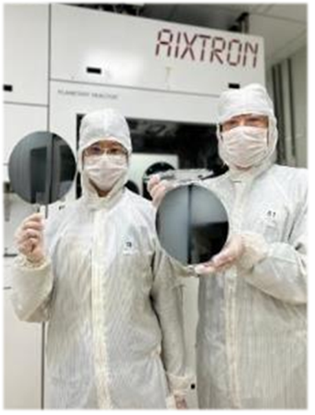
Our GaN epitaxy capabilities support growth on Si, SiC, SOI, and GaN substrates, from partial wafers up to 8-inch wafers. We provide small-batch validation and data analysis to speed up material qualification and development cycles. For power devices, our focus includes 650 V D-mode and E-mode structures with support for multi-finger layouts, aligning with industry specifications.
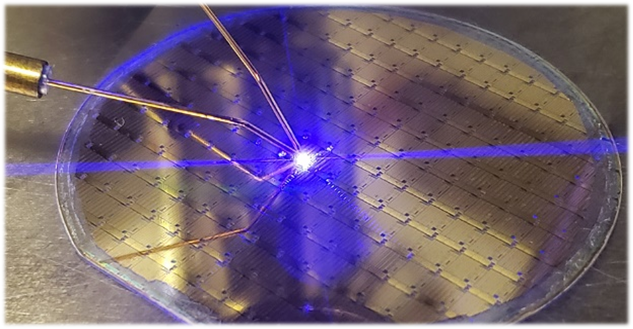
In the field of high-performance VCSELs, our team is a pioneer in GaN-based technology in Taiwan, having achieved the first successful demonstrations of blue and green VCSEL lasing. These compact, easily arrayed devices have been successfully applied in biomedical sensing, AR displays, and holographic communication. We look forward to deepening our core technologies and joining hands with partners to shape the future of GaN applications in the semiconductor and optoelectronic industries..
Photos
Contact
Name:蔡婷舜
Phone:03-5914480
E-mail:tstsai@itri.org.tw