化合物半導體與車用應用
Compound Semiconductors & Automotive Applications
Technology of the Cutting Semiconductor by Electrical Discharge Machining
Technical Features
Technology of the cutting semiconductor by Electrical Discharge Machining (EDM) uses a wire electrode to perform electrical discharge machining on semiconductor materials. Compared to diamond wire cutting, it offers advantages such as better wafer surface quality, faster processing speed, and lower carbon emissions. It is suitable for cutting high-hardness semiconductor materials and conductive materials.
Technical Description
The mainstream method for wafer slicing is diamond wire saw. However, this approach has several drawbacks, including high energy consumption of the equipment, high carbon emissions during wire production, and unstable wafer surface quality, which still requires downstream grinding. These issues are especially pronounced when cutting compound semiconductor materials such as SiC and GaN, which are extremely hard and brittle—approaching the hardness of diamond—making diamond wire saw slicing inefficient.
A non-contact machining methods are being explored as alternatives to traditional contact-based cutting. Technology of the cutting semiconductor by Electrical Discharge Machining (EDM) uses a wire electrode to perform discharge-based cutting of semiconductor materials. Compared to diamond wire saw, EDM offers advantages such as superior wafer surface quality, faster cutting speed, and lower carbon emissions during production. It is suitable for processing high-hardness semiconductor and conductive materials.
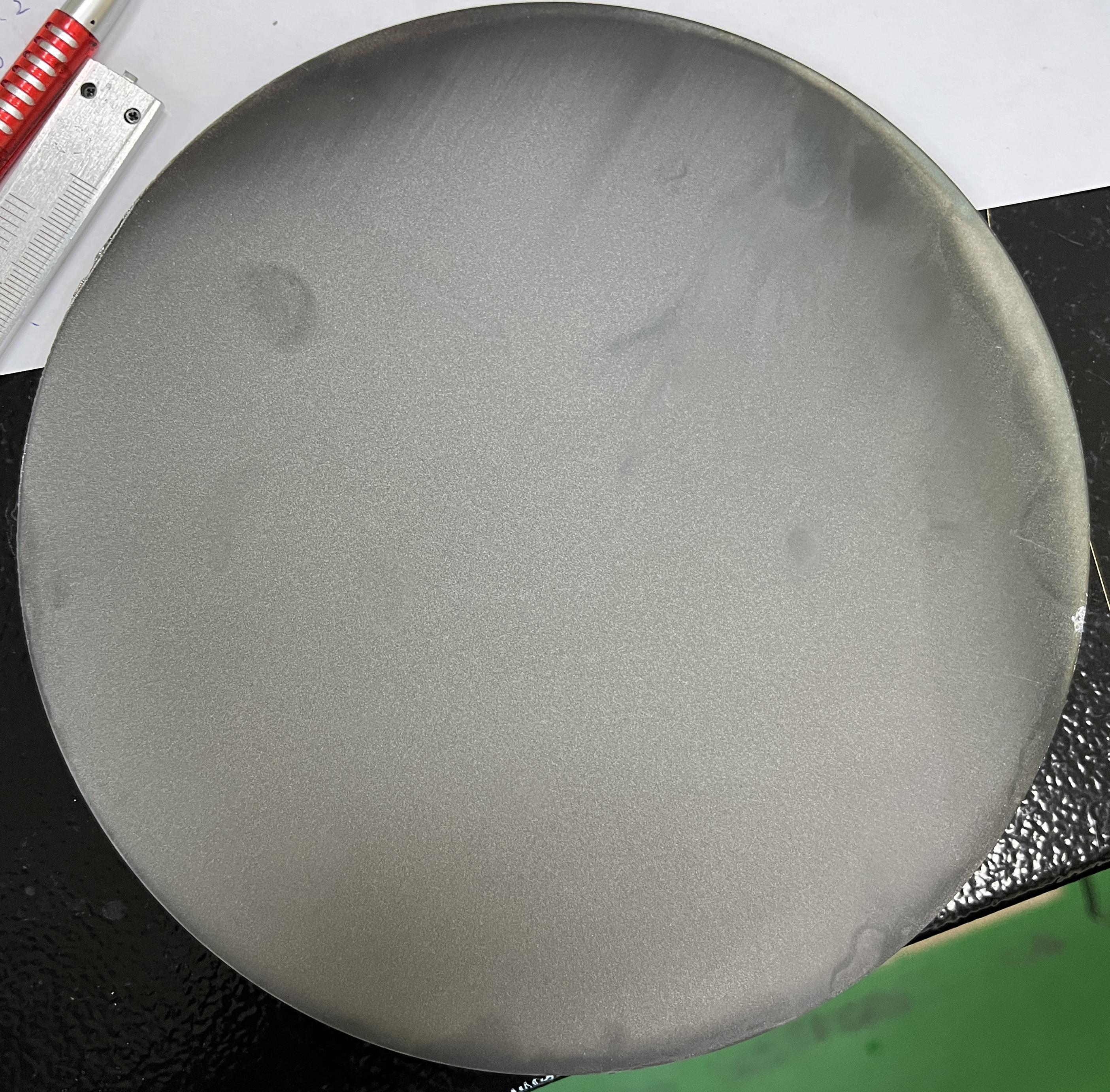
Using a single brass wire, EDM can cut an 8-inch silicon wafer at a speed of 1.25 mm/min, completing the process in approximately 2 hours and 40 minutes. The cutting surface quality is good, which helps reduce the amount of post-process grinding. This year, a multi-point EDM cutting technology is under development. That could cut multiple wafers at once, and significantly improve overall processing efficiency.
Photos
Contact
Name:陳進輝
Phone:04-23583993分機28652
E-mail:ChinHuiChen@itri.org.tw