
化合物半導體與車用應用
Compound Semiconductors & Automotive Applications
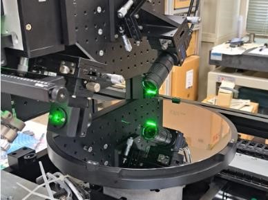
Wafer Surface Particle Detection Technology
Technical Features
Using laser scattering, all particle defects on the wafer can be quickly detected; suitable for wafers made of Si/SiC/Glass.
Technical Description
This technology is a wafer surface particle defect detection system, including an optical module and a wafer carrier. It mainly uses laser light to illuminate the wafer. If there is a particle defect on the wafer surface, scattered light will be generated; with the rotation scanning of the carrier, the particle defects on the entire wafer surface can be quickly detected and the particle position can be marked. The intensity of the scattered light is positively correlated with the particle size. As long as it is calibrated with standard test pieces of different particle sizes, the size of the particle can be obtained.
The innovation of this technology is the use of a tilted optical system and an anti-reflective carrier design. In addition to detecting opaque wafers (silicon), it can also detect transparent wafers (Glass/SiC), and has a wide range of industrial applications.
The detection system developed by this technology can provide external detection services; it can also be transferred to equipment manufacturers, who will integrate it into equipment for end customers.
Photos
Contact
Name:劉定坤
Phone:03-5743827
E-mail:teicon@itri.org.tw